This project focuses on designing an Arithmetic Unit using Verilog to implement an 8x8
multiplier, showcasing fundamental digital design principles and Verilog-based structural modeling. The
project
demonstrates how digital signal processing (DSP) techniques can be utilized in hardware for efficient
arithmetic
computations.
Key Features
- Design and Implementation: Developed a 16-bit output multiplier that
computes \( Z = \frac{1}{4} [A \times B] \), where \( A \) and \( B \) are 8-bit operands. Used an
array
multiplier design with half adders, full adders, and logical AND gates for bit-wise
multiplication
and addition.
- Core Components:
- Full Adder and Half Adder Modules: Constructed fundamental building blocks for
addition
operations.
- Shift2 Module: Designed to divide the multiplication result by 4 using right-shift
operations.
- Top Module: Integrated the arithmetic unit with a 7-segment display for real-time
result
visualization.
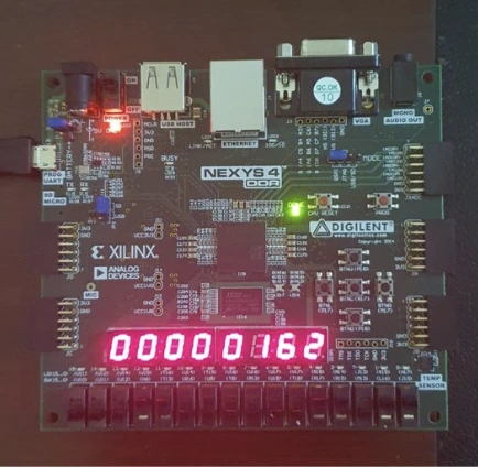
- Testing and Validation: Conducted test bench simulations to verify the design under
various
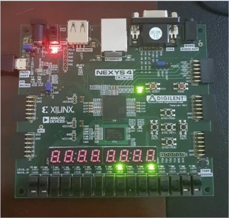
input combinations (e.g., \( A = 255, B = 255 \)). Implemented the design on an FPGA (Nexys 4 DDR board),
showcasing results on LEDs and 7-segment displays.
Project Outcomes
- Learned the principles of structural modeling in Verilog.
- Demonstrated effective use of hardware description languages (HDLs) for arithmetic operations.
- Applied the design to a real-world FPGA environment, validating its functionality.
This project highlights the significance of digital design techniques for implementing efficient arithmetic
operations, essential in DSP applications and hardware accelerators.
Technologies Used: Verilog, FPGA (Nexys 4 DDR), Vivado IDE
 | Ahmad